Noting that the Intel 4004 was normally sold as a chip set called the Intel MCS-4, the standard clock circuit used appears to be this (from this PDF, kindly provided by this vendor of MCS-4 test boards):

Which means I want to work out what this circuit is doing. First off, let’s understand these flip flops. I found this really good course on Computer Organization and Design from Intermation that I think is worth more attention that it appears to have received. I especially like how the sequence of videos starts by explaining the precursor memory types including core memory. There is of course a series of relevant Ben Eater videos as well, so I’ve linked to those as well. These concepts directly map to the flip flop usage in the Intel MCS clock circuit.
| Concept | Intermation | Ben Eater |
|---|---|---|
| Good white board descriptions of the concepts, more extensive coverage | Tangible breadboard circuits you can build | |
| SR Latches | Intermation | Ben Eater |
| Latches and Flip Flops | Intermation: Latches and Flip Flops, timings | Ben Eater: D Latches, D Flip Flops |
| Flip Flop event detectors | Intermation | |
| Flip Flop clock dividers | Intermation | |
| Building a binary counter with Flip Flops | Intermation | |
| Transparent latch applications | Intermation |
As a bonus, a dude named Brek on YouTube built his own core memory, but the only documentation I can find is a series of YouTube videos from 2015. Certainly the links in the Hackaday article are all 404 errors now. I made a playlist of just those videos for convenience.
So, this circuit starts to look like two clock dividers based on watching all those videos. Here’s the top half of the circuit redrawn in LTSpice:

Note that I am using LTSpice on a Mac, which doesn’t have a toolbar. This makes it much harder to use, especially if you don’t really know what you’re doing like me. This LTSpice for Mac YouTube tutorial really helped me out here. It doesn’t help that LTSpice on the Mac seems to be quite buggy and wouldn’t actually save my edits unless I snuck up on them (hot tip, pay attention to encoding and end of line characters if you end up just wanting to edit the .asc file in a text editor). I also needed these settings for each of the D flip flops to make the simulation work:

Which meant we could finally visualize the output of this clock circuit, which turns out to be a multi-phase clock divider:

This maps to what the MCS-4 manual from 1973 says:
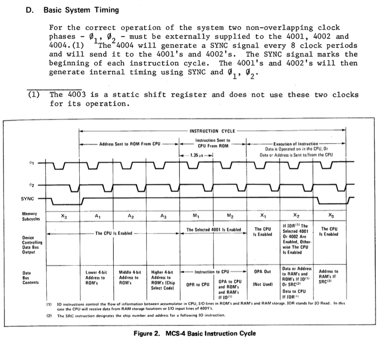
Note that the MCS-4 is super into active low pins, so you need to mentally flip this timing diagram. Its basically saying that CLK1 and CLK2 alternate, and then after 7 cycles of that you get a single cycle of CLK1, CLK2, and SYNC. This is done because addresses and data are multiplexed across only four pins on the chops to keep pin counts down. SYNC is generated internally in the 4004 based off of CLK1 and CLK2.
So anyway, baby steps to understanding some of the Intel 4004 circuitry a little better.